Navitas Unveils GaN Half-bridge ICs with MHz Switching
In the field of power electronics, one of the most sweeping changes today is the proliferation of wide-band gap semiconductors. Replacing legacy silicon FETs, new materials such as silicon carbide (SiC) and gallium nitride (GaN) are helping engineers achieve greater performance, efficiency, and reliability in power circuits.
Despite the benefits of these materials, the field is still relatively young and there is much maturation still needed. Today, Navitas Semiconductor is addressing some of these challenges with the announcement of its new GaN-based half-bridge IC solutions.
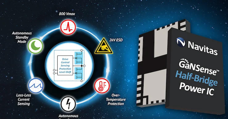
Navitas has released a new family of half-bridge GaN devices.
Navitas has released a new family of half-bridge GaN devices. Image used courtesy of Navitas Semiconductor
All About Circuits had the chance to talk with Llewellyn Vaughan-Edmunds, senior director of marketing at Navitas Semiconductor, to hear about the new product firsthand.
GaN and the Need for Integration
Of the emerging wide-bandgap semiconductors, GaN is one of the most exciting. Namely, GaN offers a device structure with less parastics, a low RDS(on), inherently faster switching speeds, and higher breakdown voltages than its silicon equivalent.
However, owing to its unique nature and speed, GaN can be considerably difficult to drive and control. Because of this, to optimally work with GaN often requires a dedicated gate driver IC that is specifically developed for GaN, including proper circuit design such as power routing, gate-loop routing, and decoupling. Here, the best way to achieve this high performance is through the integration of the gate drive and the GaN FET on the same IC.
“What differentiated Navitas from the other GaN companies is that we integrated a gate driver with the power stage monolithically,” says Vaughan-Edmunds. “This not only helps you to switch a lot faster, but also to regulate and protect the very sensitive gate on GaN, which has reliability concerns. But if you can put this driver together with the gate driver, then that takes out all the way.”
However, the need for integration does not stop here. Integrating a GaN driver and a GaN FET onto a single IC helped unlock maximal performance for single-device switching applications, but in practice, power electronics often rely on the operation of more than one FET.
Specifically, the two-transistor half-bridge topology is amongst the most universal in power electronics, finding applications such as motor drivers and inverters. Here, like elsewhere, maximum performance can only be unlocked by higher levels of integration.
Navitas’ Half-bridge GaN Solution
Today, Navitas Semiconductor addressed these issues with the announcement of its new family of fully-integrated half-bridge GaN IC. The device moves this class of devices out of the kHz realm and into MHz switching frequencies, according to the company.
Vaughan-Edmunds begins telling us “The half-bridge is a fundamental block in power electronics. So what Navitas has done is put the two switches inside this one package solution, a 6x8 PQFN, low inductance, industry-standard package.”
The new family, which is highlighted by the flagship NV6247, is said to benefit greatly through the integration of the half-bridge onto a single IC. Specifically, Navitas tells us that they are able to achieve faster speeds, greater reliability, and overall better performance than with a discrete solution. Beyond this, the integration of the half-bridge enables a significant reduction in BOM and design complexity as compared to discrete solutions.
Vaughan-Edmunds further explains the benefits of integration, saying that the integration of the half-bridge results in a decrease in the amount of circuits, circuitry, PCB, space and components required.
High-integration reduces footprint but also boosts performance.
High-integration reduces footprint but also boosts performance. Image used courtesy of Navitas Semiconductor
“By switching over to the half bridge, you reduce everything by over 60% fewer components, more than 60% on the footprint size, and you completely integrate everything now,” he says.
“When you’re switching these devices in a discrete way, there's a lot of noise and this affects reliability and the gate performance. By integrating everything, you can move to a very efficient, smooth switching way in the circuit. So the key is integration. Integration means high speed.”
The NV6247 is rated at 650 V, 160 mΩ (dual), but the GaNSense Half-Bridge ICs family includes a second device, the NV6247C, which is rated at 275 mΩ (dual). Both chips are provided in an industry-standard 6x8 mm PQFN package.
The NV6247 is available now in production, while the NV6245C is sampling to select customers. The NV6245C will be broadly available in production to all customers in Q4 2022, says the company. More information is available in Navitas’ application note AN018.
What’s the Industry Impact?
GaN is still an emerging technology and, as such, has a lot of room for growth and improvement. With Navtias’ new family of integrated half-bridge GaN devices, the company is seemingly pushing the field in the right direction—driving greater performance and simplicity for the design engineer.